


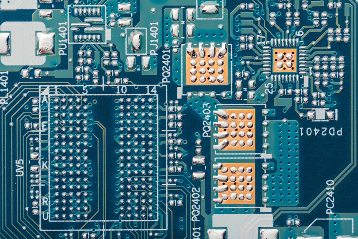
Printed circuit boards (PCBs) are one of the most significant waste streams within Waste Electrical and Electronic Equipment (WEEE). They are found in virtually every electronic device, from computers, mobile phones, and televisions to household appliances, servers and industrial equipment. Due to the continuous increase in the consumption of electronic devices and the shortening of their service life, the generation of PCB waste continues to grow. This article provides an introduction to PCBs as a waste stream, explains why their recycling represents such a major challenge, and discusses how mechanical, chemical and biological recycling approaches are currently being applied.
PCBs are among the most important fractions within electronic waste because, although they represent a relatively small proportion by weight, they contain a significant share of the metallic value of electronic equipment. Their recycling is complex because they consist of a highly heterogeneous mixture of materials, including fiberglass-reinforced resins, conductive copper layers, solder joints, and numerous electronic components.
In general terms, a PCB can be divided into three main parts: the non-metallic substrate, the conductive metallic layers, and the surface-mounted components. This distinction is crucial for recycling, as not all fractions have the same value or require the same treatment. The metallic fraction and certain electronic components represent the primary targets for the recovery of valuable and critical materials.
From a resource recovery perspective, the metallic fraction of a PCB is mainly composed of copper, which is generally the dominant metal in conductive tracks, together with tin, nickel, iron, aluminum and smaller quantities of precious metals such as gold, silver and palladium. In addition, certain components mounted on the PCB—including capacitors, connectors, integrated circuits, microchips and metallic contacts—may contain elements of particular interest, such as tantalum, cobalt, and even small amounts of rare earth elements, depending on the type of equipment. Consequently, both the metallic portion distributed throughout the PCB and specific electronic components constitute the main focus of recycling efforts because they contain a large share of the recoverable value of the waste.
Why are PCBs a recycling challenge?
The main difficulty associated with PCB recycling stems from their high level of complexity. Unlike more homogeneous waste streams, all materials within a PCB are intimately bonded together. Metals do not appear as easily separable pieces but rather as thin layers, solder joints, conductive tracks, or miniature components. As a result, simple and clean separation is extremely difficult, complicating the efficient recovery of high-value materials.
Furthermore, the motivation for recycling PCBs is not solely economic but also environmental and strategic. On the one hand, inadequate management can lead to the release of hazardous substances and the irreversible loss of valuable metals. On the other, many elements present in electronic waste are essential for the technology industry and the energy transition, while their primary supply is concentrated in only a few countries. The Global E-waste Monitor 2024 highlights that only around 1% of rare earth demand is currently met through electronic waste recycling, illustrating the significant gap that still exists between the potential of these waste streams and actual recovery rates.
Another important aspect is that not all PCBs are alike. Their composition varies significantly depending on the type of equipment from which they originate. A smartphone PCB differs substantially from that of a server, power supply, or industrial machine. This variability complicates the design of universal recycling processes, as metal concentrations and the presence of valuable components can differ greatly from one waste stream to another.
How are PCBs currently recycled?
PCB recycling is generally approached as a combination of several processing stages. Initially, dismantling, shredding, and sorting operations are applied to liberate materials and concentrate the metallic fraction. Subsequently, thermal, chemical, biological or combined treatments are applied to the enriched fractions, depending on the target metals and desired recovery objectives.
Recent scientific literature emphasizes that the future of PCB recycling lies not in indiscriminate shredding of the entire waste stream, but rather in working with increasingly selected and enriched material streams. This approach improves both technical efficiency and economic viability.
Mechanical recycling
Mechanical recycling is continuously evolving through the incorporation of advanced technologies from fields such as artificial vision and artificial intelligence. Traditionally, mechanical recycling relied on shredding and physical separation processes designed to produce metal-enriched fractions. However, current trends focus on more selective and efficient strategies capable of maximizing the recovery of high-value materials.
In this context, identification systems based on cameras and machine-learning algorithms are being developed to classify PCBs according to their composition, typology or morphological characteristics. Through the creation of appropriate databases and the training of models using representative datasets, it becomes possible to generate more homogeneous waste streams, significantly facilitating subsequent recovery and recycling stages.
Likewise, machine vision technologies offer new opportunities for the identification and selective extraction of high-value electronic components present on circuit boards. This capability not only increases the efficiency of critical and strategic material recovery but also contributes to the automation of processes that have traditionally been challenging due to the high heterogeneity of electronic waste.
Mechanical recycling also plays a key role as a complementary step to other recovery technologies, such as chemical and biological processes. Its main function is to condition and concentrate target materials, generating streams better suited for subsequent treatment. In this way, different recycling technologies can be integrated into circular economy schemes, particularly when a single treatment route is insufficient to achieve the required recovery rates.
Chemical recycling
Chemical recycling of PCBs is primarily based on hydrometallurgical processes, that is, techniques that dissolve the metals contained in the PCB and subsequently recover them selectively. Unlike purely mechanical treatments, which only separate materials physically, hydrometallurgy acts on the chemical composition of the waste and enables the production of metal-bearing solutions from which individual elements can be purified and recovered.
For this reason, chemical recycling is currently considered one of the most important routes for PCB resource recovery, particularly for the recovery of critical raw materials (CRMs).
Following the mechanical pre-treatment stage, a leaching process is applied using reagents capable of dissolving the metals. Common systems include acidic media such as sulfuric acid or hydrochloric acid, typically combined with oxidizing agents to improve metal dissolution.
Alternative leaching systems to conventional mineral acids are also being investigated, particularly organic acids and deep eutectic solvents (DES). These approaches have attracted increasing interest because, in certain cases, they can improve process selectivity while reducing some of the drawbacks associated with the intensive use of conventional reagents. However, their industrial implementation remains more limited than that of traditional hydrometallurgical systems.
After leaching, dissolved metals must be separated and purified. Various techniques are employed, including selective precipitation through pH adjustment, solvent extraction, adsorption, electrodeposition, and, in some studies, ionic liquids. The combination of these stages allows different metals to be sequentially recovered in the form of salts, concentrates or refined metals with sufficient purity to be reintroduced into new value chains.
The main advantage of this route lies in its selectivity, as separation schemes can be tailored to the specific composition of the waste stream. However, this selectivity also constitutes one of its principal challenges. PCBs contain many different elements, and poorly optimized leaching may result in the simultaneous dissolution of metals that are difficult to separate later. Furthermore, reagent consumption, liquid effluent generation, and purification costs mean that the process must be carefully optimized to achieve technical and economic viability. Consequently, current research focuses not only on maximizing recovery rates but also on reducing reagent consumption, minimizing secondary waste generation, and improving overall sustainability.
Biological recycling
Biological recycling of PCBs, also known as bioleaching, is emerging as an alternative to conventional chemical processes. It exploits the ability of certain microorganisms to promote the dissolution of metals contained within the waste, making them available for subsequent recovery.
The microorganisms most commonly used in these processes are acidophilic bacteria capable of oxidizing iron, such as Acidithiobacillus ferrooxidans. These microorganisms generate acidic conditions and oxidizing species that facilitate the dissolution of metals present in PCB metallic fractions. In general, metal solubilization can occur through acidolysis, driven by the protons or acids generated by microbial metabolism, or through redox mechanisms that contribute to metal dissolution.
In addition to bacteria, fungi such as Aspergillus niger have also been studied because of their ability to produce organic acids that promote metal dissolution. This approach is particularly interesting because it could potentially be integrated with low-cost carbon sources or even organic waste streams, adding a further circular economy dimension to the process.
The main advantage of biological recycling is its potentially lower environmental impact, as it reduces the need for aggressive chemical reagents and operates under milder conditions. However, significant challenges remain, including longer processing times, slower reaction rates, sensitivity to waste toxicity and scale-up difficulties. Consequently, biological recycling is currently viewed as a promising complementary technology rather than a direct replacement for established chemical routes.
Conclusions
Printed circuit boards represent one of the most complex and valuable fractions within electronic waste due to both the diversity of materials they contain and the presence of economically and strategically important metals. Recycling PCBs presents significant technical challenges because these waste streams combine metallic, non-metallic and electronic fractions with different characteristics and compositions.
As a result, effective PCB valorization requires complementary approaches capable of addressing this complexity. In this context, the development of diverse recycling routes, together with advanced separation and sorting stages, is essential for achieving more efficient, selective and sustainable processes. Such advances will enable greater value recovery from PCB waste while strengthening the role of electronic waste recycling within a circular economy framework.
Javier Castillo, Javier Grau and Max Torrellas are Recycling, Recovery and Biotechnology researchers at AIMPLAS